India’s Semiconductor Diplomacy Beyond Manufacturing: Can Strategic Partnerships Deliver Technological Sovereignty?

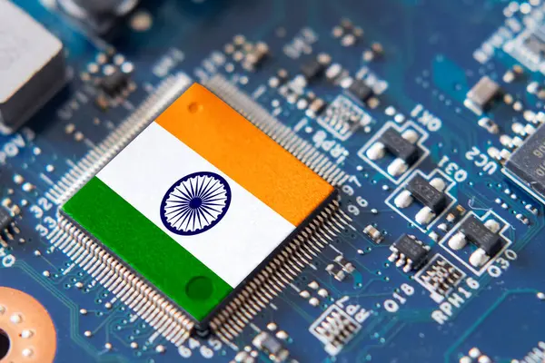
India’s semiconductor policy for the past five years was mostly that of an industrial policy, with semiconductors being in the form of subsidies, fabs, and employment. That framing is now outdated. As the India Semiconductor Mission (ISM) moves into its second phase with a proposed outlay of roughly $13 billion which is more than 60 percent above the first phase’s $10 billion allocation India’s chip ambitions have become as much a diplomatic project as an industrial one. However, Washington, Tokyo and Taipei have each woven semiconductors into more comprehensive “economic security” architectures with New Delhi in the past eighteen months. Raising the question for India is not whether it can attract capital and fabs, but can it build a strategy to get them based on foreign technology transfer, equipment and design tools and still plausibly achieve the “technological sovereignty” that Indian officials are increasingly invoking.
From subsidy scheme to strategic architecture
The manufacturing figures are indeed important. So far, the government has sanctioned 13 semiconductor and display projects in seven states totalling an investment pipeline of approximately ₹1.64 lakh crore (about $17 billion), comprising one large logic chip plant, 13 compound semiconductor plants and nine packaging plants. In February 2026, the mission’s first operational plant in Sanand was inaugurated, and the ISM 2.0, approved by the Expenditure Finance Committee of the Finance Ministry in early July, is specifically aimed at moving beyond assembly and packaging to equipment, materials and the development of indigenous chips.
What has changed is the diplomatic scaffolding around this build-out. The large-scale fab or packaging project isn’t a standalone commercial deal but is now part of a bilateral or minilateral agreement.
The US pillar: TRUST and its fragility
The U.S. is India’s most structured semiconductor partner. In February 2025, the 2022 Initiative on Critical and Emerging Technology (iCET) was expanded to TRUST (Transforming the Relationship Utilizing Strategic Technology), which includes semiconductors, AI infrastructure, critical minerals, quantum computing, and defense-industrial cooperation. The architecture has resulted in tangible results so far, including the memorandum of understanding in 2023 linking the CHIPS and Science Act to ISM, the Bharat Semi–3rdiTech “Shakti” fab for defence-grade gallium nitride and silicon carbide chips with the US Space Force, and continued investments in India by Applied Materials and Lam Research in training centers and R&D facilities.
However, as the Center for Strategic and International Studies noted, the advancements are happening “in the face of new trade and tariff uncertainties,” a nod to the Trump administration’s periodic threats of imposing high tariffs on semiconductor imports, a move that doesn’t sit well with the TRUST initiative’s cooperative spin. The analysts at the Pacific Forum have also warned that the imperative to develop US-India semiconductor relationships has to be actively reworked because the path is not guaranteed but it is “fragile.” The core of this ideology is that sovereignty is based on a single great-power alliance and is the fact that it is only as enduring as the political climate in Washington.
Taiwan and Japan: filling the technology-transfer gap
The US connection provides the political cover and the component of capacity with defense links; Taiwan provides the more difficult-to-substitute component: process know-how. According to Taiwan’s own representative office in New Delhi, it is one of the “twin pillars” of bilateral cooperation, along with the Foxconn-HCL display-driver joint venture in Uttar Pradesh, as the joint venture between Tata Electronics and Powerchip Semiconductor Manufacturing Corporation (PSMC) in Dholera in Gujarat is India’s first 300mm wafer fab and is backed by approximately $11 billion dollars in investment. According to Taiwan Insight, thousands of Indian engineers have been sent to work in Taiwan at semiconductor facilities, such as Hsinchu Science Park, since the informal Taiwan-India Semiconductor Alliance was formed in 2024, and new academic ties are building on this pipeline. This is a real transfer of tacit manufacturing discipline, something that India could not easily emulate by capital alone and, by definition, a dependence: India’s most advanced fab is the result of a Taiwanese company deciding to licence its process technology.
Japan’s involvement has been redefined even more explicitly in terms of security. In July 2026, just before the visit of Prime Minister Sanae Takaichi to New Delhi for the first time as premier, the two governments signed a Joint Declaration on Economic Security Cooperation with regard
to semiconductors, critical minerals, ICT, clean energy and pharmaceuticals, with the parties referring to “economic coercion and non-market policies and practices” clearly targeted at China’s dominance over rare-earth and mineral supply chains. Under ISM 2.0, the declaration pledges Japan to participate more actively and also technical cooperation is to be provided between the Geological Survey of India and Japan’s JOGMEC in the mineral processing field. Notably, one Indian commentator in response to the announcement reflected a common skepticism: such statements have been coming for years, and progress on the ground has been “slow” . A cautionary note: joint statements are a primary indicator, NOT a lagging one, of capability.
What “sovereignty” still lacks
Manufacturing capabilities and true sovereignty are best compared by what these partnerships don’t cover. The Tata-ASML agreement signed in May 2026 to supply the Dholera fab with extreme ultraviolet lithography systems is evidence of India’s reliance on a single supplier from the Netherlands, a chokepoint controlled, in part, by Washington. The software tools that help designers create the chips before they are manufactured are still controlled by a few U.S. companies, known as electronic design automation (EDA) software. And India’s semiconductor supply chains are no exception: they depend on gallium, germanium and rare earths that are processed by the Chinese and the very “arbitrary export restrictions” the India-Japan declaration refers to as a systemic risk but hasn’t been addressed yet.
The India Roadmap, released by the National Institution of Transforming India (NITI Aayog) in May 2026, is clear that India wants to design and manufacture chips for only 70-75 percent of its consumption by 2029, not to claim to be at the forefront of chip fabrication or tools. That’s a good, attainable goal, but it is not the same as sovereignty in terms of having sovereignty over the entire value chain.
Conditional sovereignty, not autonomy
None of this is a failure of India’s semiconductor diplomacy, but rather the confirmation that it is indeed not an autarky approach but one of “trusted redundancy”. One by one, each partnership makes a single foreign dependency into a diversified, allied dependency: American defense-related capacity, Taiwanese process know-how, Japanese mineral and ICT cooperation. This is likely to provide resilience and a significant portion of the global packaging and legacy-node manufacturing capacity. But on current trends, it can’t yet create and manufacture the cutting-edge chip without relying on foreign lithography equipment, foreign design software, and foreign refined materials.
The proper term for policymakers, therefore, is conditional sovereignty: control of a sufficient portion of the value chain to be free from coercion, within a system of alliances that in turn is subject to political risk from tariff wars to changing export-control regimes. The durability of that will depend on how well the declared shift toward equipment, materials and indigenous IP in ISM 2.0 withstands the test of contact with the reliable power supply, harmonized standards and the streamlining of regulations identified by the CSIS analysis as still-pending bottlenecks despite three years of diplomatic progress.
The views and opinions expressed in this article are those of the author(s) and do not necessarily reflect the official policy or position of the International Dialogue & Diplomacy Foundation (IDDF).